


Because 2D NAND’s ability to shrink is reaching its limits, the NAND industry has been working for a few years on 3D, which is expected to enable the flash memory industry to continue the Moore’s Law trend by increasing bit density and GB capacity of any given silicon area (see chart 1). In addition to being higher density, 3D NAND is expected to offer higher performance, better reliability and lower power use than 2D. With its improved capabilities, 3D also can boost existing applications and enable new ones. This article discusses the differences between 2D NAND and 3D NAND and describes various applications and cases in which 3D is a better choice. (It is important to note that 2D NAND is a mature technology that holds its own attributes and is expected to support various applications for the foreseeable future in coexistence with 3D NAND.)
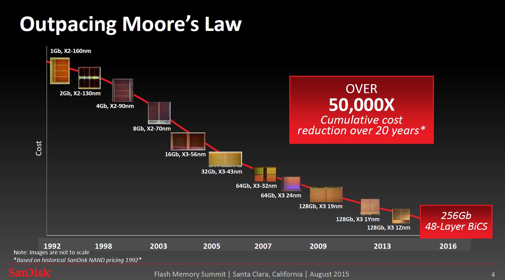 Chart 1: 3D NAND continues Moore’s Law (Source: SanDisk, Flash Memory Summit Presentation 2015)
Limitations of 2D Planar NAND
Patterning challenge
Patterning is a photolithography process in which light is used to transfer a geometric pattern from a mask to a photoresist on a chip to eventually create electrical circuits. The current lithography tool is unable to generate a light wavelength that can draw the finer geometries needed, so costly and repeated patterning steps are used. For example, a 15-nanometer (nm) cell requires quadruple patterning, which increases cost and complexity. Effective shorter wavelength light equipment is not yet available for high-volume manufacturing; therefore, the sub-15-nm class process cost and reliability become challenging. 3D NAND is designed to be more cost-effective because it can choose the correct number of layers, as will be explained next.
Cell-to-cell interference
Technical challenges of continued shrinking arise when an electrical charge in a cell affects its adjacent cells, creating cell-to-cell interference (a.k.a., proximity effect), which may lead to errors and data corruption. When a cell is less than 15 nm, the chance of interference increases, making the cell less reliable.
3D NAND Memory Technology
3D NAND technology achieves high density by stacking layers of cells on top of each other in a vertical NAND string structure, rather than shrinking the cells at the planar level. This way, higher bit density is achieved for a smaller footprint, and the lithography patterning limitation is eliminated.
Capacity increase with additional layers
In the near future, 3D will be constructed of 48 layers of memory cells that are connected in a vertical NAND string through a cylindrical channel (see chart 2). With additional development, it may be possible in a few years to exceed 100 layers, dramatically boosting capacity and density. This structure simplifies the costly repeated patterning steps, but creates other challenges due to its vertical structure.
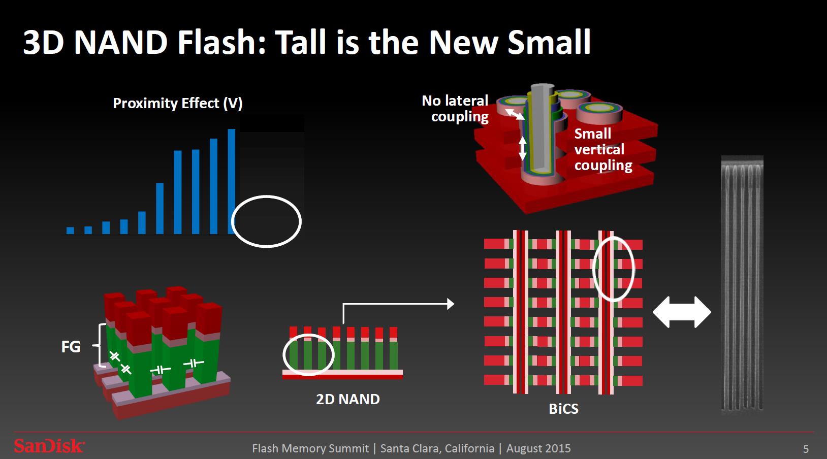
Chart 2: Tall is the new small (Source: SanDisk, Flash Memory Summit Presentation 2015)
Charge Trap Material
SanDisk and several other flash makers use Charge Trap Layer (CTL) rather than the electrically conductive Floating Gate (FG) used in 2D NAND. CTL is a non-conductive layer that acts as an insulator and, along with other memory cell features, is designed to reduce cell-to-cell interference, lowering the number of errors and increasing reliability margins. A representation of the CTL memory cell is shown in chart 3.
The non-conductive properties of the Charge Trap Layer also allow for less complex patterning production flow.
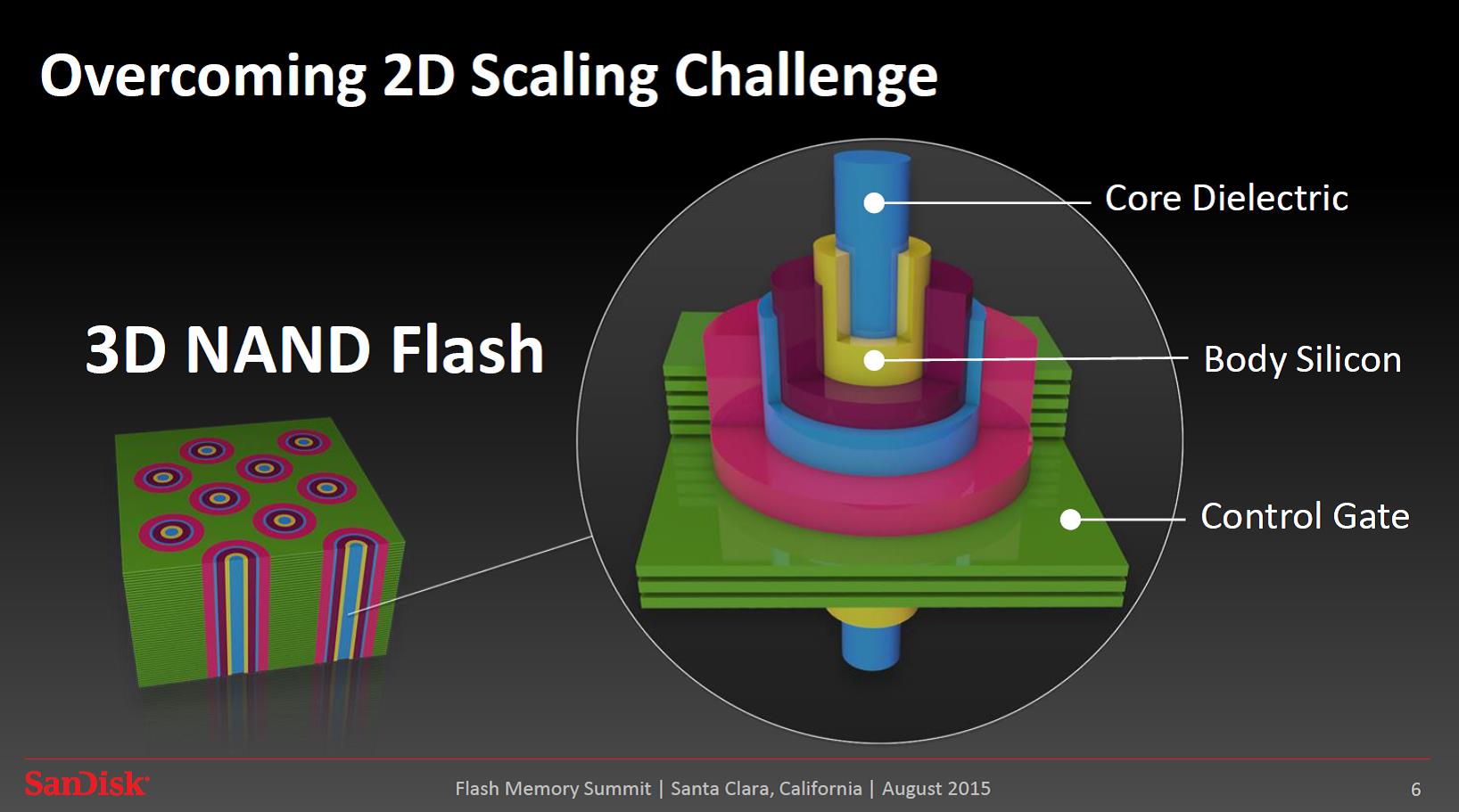 Chart 3: SanDisk’s memory cell (Source: SanDisk, Flash Memory Summit Presentation 2015)
Higher endurance due to lower cell-to-cell interferences (proximity effect)
The number of program/erase cycles (a.k.a., endurance) of a NAND flash memory chip is affected by the electrical fields produced by the charge stored in the memory cell. Higher electric fields can create interferences with the adjacent cells, which in turn lowers the chip’s endurance. The Charge Trap material of 3D NAND, along with relaxed design rules (larger cell critical dimensions), more electrons stored in the larger cell and optimized circular cell design, all improve the number of program/erase cycles and allow more terabytes written (TBW) over a longer period of time.
Faster performance through simpler program algorithm
NAND flash programming speed is affected by the complexity of the program algorithms that write the data. 2D planar NAND flash requires very precise sets of complex program algorithms to prevent errors created by cell-to-cell interference. These complex algorithms require additional time for data to be written, resulting in slower speed. Because 3D NAND technology is less sensitive to cell-to-cell interference, it can write data significantly faster, resulting in better performance.
Less power consumption due to simpler programming operation
To neutralize the effects of cell-to-cell interference, traditional 2D planar NAND flash must perform a greater number of programming steps, which increases power consumption. Because 3D NAND technology has reduced interference, the number of programming steps has been vastly reduced, and so, along with other improvements, power consumption will be substantially lower.
Markets and Applications
Examination of the performance, power, reliability and storage capacity requirements for various applications reveals that 3D NAND can be a better choice, especially in imaging/removables, enterprise and client SSDs, and embedded memory in mobile devices.
In imaging applications, flash memory used in surveillance cameras (continuous video recording) requires a large memory capacity to store massive amounts of data with high endurance. For instance, failure of a flash device located on top of a surveillance tower can cause inconvenient interruption and result in a costly repair; therefore, it is important that such a system offers high reliability. The various professional action cameras available today are another example that requires high performance and large capacity.
Solid state drives (SSDs) require high storage capacity, high performance and high endurance, and for the more demanding use cases, 3D NAND is expected to be a better solution.
Mobile devices such as smart phones, tablets and phablets require high performance, small form factor, low power and high endurance, all driven by the demand for enhanced user experience. This is because of higher numbers of, and higher resolution in, video/pictures; higher processing due to the number of cores and new OS; RAM-to-flash swap; high sequential read speed for booting; high sequential write speed for side loading and more. Tablets and phablets in particular require ever-increasing storage capacity, but at a very low cost. The latest version of Android, Marshmallow, creates the opportunity for external memory cards to function as storage for application execution, creating an additional driver for high-performance memory cards.
Connected home systems require high memory capacity and high endurance to support functions such as time shift buffer (TSB), video caching, content prefetching, data storage and applications. These systems are designed for an extended lifespan of five to seven years, thus requiring high reliability.
In the automotive industry, flash memory plays a growing role in infotainment, connected cars, autonomous driving and driver assistance. Large amount of data are continuously collected and processed by the many sensors in these subsystems, which need to be highly reliable in a wide range of temperatures and, when aggregated, also require high capacity.
Interfaces such as UFS and PCIe support the higher data speeds and parallel execution that can better take advantage of the improved flash capabilities. These capabilities also can enable new applications such as cold tier storage replacement and large disaggregated enterprise storage.
Summary
3D NAND’s expected continuation of cost reduction for several generations as well as its improved capabilities make it the preferred option for more demanding requirements over time. Due to its high-bit density, the cost advantage of 3D NAND over 2D will be better demonstrated in cases where high storage capacity is required.
Coexistence with 2D NAND is expected, as 2D still addresses a broad array of applications and a good portion of worldwide fab output will remain 2D for years to come.
©SD Association. All rights reserved. SD, SDHC, miniSDHC, microSDHC, SDXC and microSDXC Logos are trademarks of SD-3C LLC
Avi Klein is a Senior Principal Device Engineer, managing the device team at SanDisk in Israel. In this role, Klein conducts research studies, characterization and qualifications of Flash Memory for the specific needs of the mobile market. Klein has more than 30 years of experience in the semiconductor industry. He can be reached at Avi.Klein@SanDisk.com.
The views expressed in this article are those of the author and not necessarily those of SanDisk.